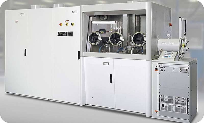
Metal-organic chemical vapor deposition (MOCVD). Courtesy of the Electronics and Telecommunications Research Institute (ETRI).
South Korean researchers have succeeded in developing mass production technology for quantum dot lasers, which are widely used in data centers and quantum communications, a breakthrough that paves the way for cutting the production costs of semiconductor lasers to one-sixth of the current level.
This study Alloys and Compounds Journal.
The Electronics and Telecommunications Research Institute (ETRI) of Korea has announced that it has developed the first mass-production technology in Korea for quantum dot lasers, which have previously only been used for research purposes, using a metal-organic chemical vapor deposition (MOCVD) system.
ETRI’s Optical Communication Components Research Division has successfully developed an indium arsenide/gallium arsenide (InAs/GaAs) quantum dot laser diode on a gallium arsenide (GaAs) substrate suitable for the 1.3 µm wavelength band used in optical communications.
Conventionally, quantum dot laser diodes have been manufactured using the molecular beam epitaxy (MBE) method, but this method is inefficient due to its slow growth rate, making mass production difficult. The research team has significantly improved the productivity of quantum dot laser manufacturing by utilizing the highly efficient MOCVD method. Quantum dot lasers are known for their excellent temperature characteristics and strong resistance to substrate defects, and can be manufactured over a larger substrate area, reducing power consumption and manufacturing costs.

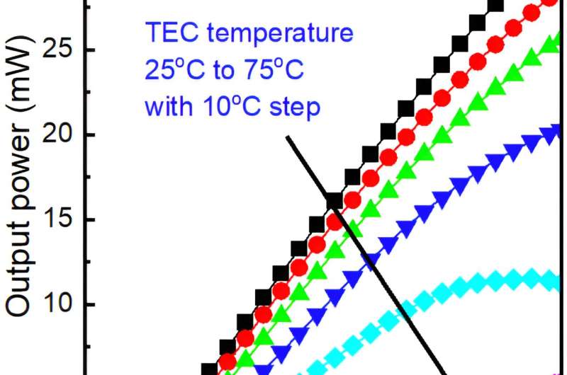
High temperature (75°C) operation data for quantum dot lasers. Source: Electronics and Telecommunications Research Institute (ETRI).
The quantum dot manufacturing technology developed this time has excellent density and uniformity, and the quantum dot semiconductor laser produced has been demonstrated to operate continuously up to 75°C, making it one of the world’s best results achieved using MOCVD.
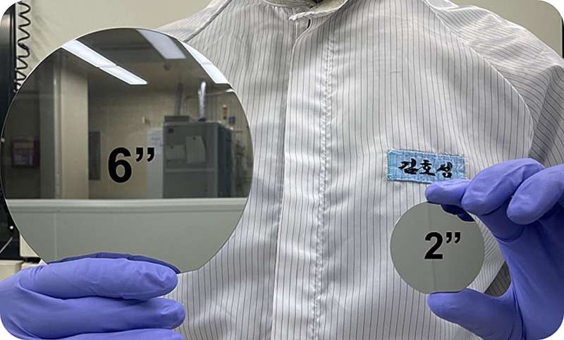
Traditionally, optical communication devices have used expensive 2-inch indium phosphide (InP) substrates, which make them expensive to manufacture. A new technology that uses GaAs substrates, which are less than one-third the cost of InP substrates, is expected to reduce the manufacturing cost of communication semiconductor lasers by more than one-sixth.
This technology allows the use of large area substrates, significantly reducing process time and material costs.
The research team plans to further optimize and validate the technology to increase its reliability and then transfer it to domestic optical communications companies, who will receive key technical and infrastructure support through ETRI’s semiconductor foundry to accelerate their commercialization timeline.

Comparison of 2-inch and 6-inch compound semiconductor substrates. Courtesy of the Electronics and Telecommunications Research Institute (ETRI).
The shortened development period and reduced production costs are expected to make the products more price competitive and expand market share internationally. This progress is expected to revitalize the domestic optical communication components industry.
Optical communications are the backbone of industry in modern society, and the research team’s findings will revolutionize the development of light sources that connect apartment complexes to large cities and undersea optical cables.
Professor Dae Myung-geum of Chungbuk National University, who was involved in the research, said, “The mass production technology of quantum dots will drastically reduce the production costs of expensive optical communications equipment, increase the competitiveness of the domestic optical communications parts industry, and make a great contribution to basic scientific research.”
“This research result is a great example of ensuring both commercial viability and radical innovation, and has the potential to change the paradigm of the semiconductor laser industry for optical communications,” said Dr. Ho Sung Kim from ETRI’s Optical Communications Components Research Division.
For more information:
HoSung Kim et al., High-temperature continuous-wave operation of all-MOCVD-grown InAs/GaAs quantum dot laser diodes with highly strained layers and low-temperature p-AlGaAs cladding layers, Alloys and Compounds Journal (2024). DOI: 10.1016/j.jallcom.2024.173823
Provided by the National Science and Engineering Research Council
Quote: Researchers develop technology to mass-produce quantum dot lasers for optical communications (June 28, 2024) Retrieved June 28, 2024 from https://phys.org/news/2024-06-technology-mass-quantum-dot-lasers.html
This document is subject to copyright. It may not be reproduced without written permission, except for fair dealing for the purposes of personal study or research. The content is provided for informational purposes only.

